Making analog-to-digital converters for digital ultrasound probes
Making good digital ultrasound probes is extremely challenging because of the constrained amount of power that can be used. If significantly more than a couple of watts are consumed, the probe gets too hot to be allowed to touch your skin. When thousands of parallel ultrasound transmitters and receivers are preferred in a 3D ultrasound probe, it becomes clear that this power budget is tough.
In an ultrasound system, the handheld probe is the part that transmits ultrasound pulses into your body and captures the echoes. The probe tip has a number of transducer elements, which are tiny devices that act as ultrasound “speakers/microphones”. Normally, these elements are connected to the ultrasound machine, which converts all the echoes to digital signals used to make the image.
An alternative approach is to use a digital ultrasound probe, which converts echoes to digital signals in the probe itself. The probe can then send a digital data stream to the ultrasound machine, perhaps wirelessly. This will be a great advantage in 3D ultrasound, where the probe contains thousands of elements. It also enables the design of probes that are complete small ultrasound machines on their own, sending images to phones or tablets.
One of the most important parts of the ultrasound receivers are the analog-to-digital converters (ADCs), which convert ultrasound echoes into digital signals. In CIUS, we work on designing receiver ADCs that can be used in digital probes. These can only use a few hundred microwatts each to not exceed the power budget of the probe (one microwatt is 0.000001 watt). That is a tiny amount of power when we want to digitize the ultrasound echoes more than ten million times per second.
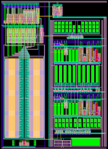
To make these low-power ADCs, we first and foremost need to make our own chips, using modern integrated circuit technology. Inside these we can have our custom designed ADCs, which we make as small and simple as possible, because smaller electronics use much less power. However, when electronic circuits are sized down, their accuracy eventually start to suffer, and we get too much noise and distortion in the ultrasound signals. The key to solving this is to figure out clever ways to reduce noise and distortion without making the circuits much larger.
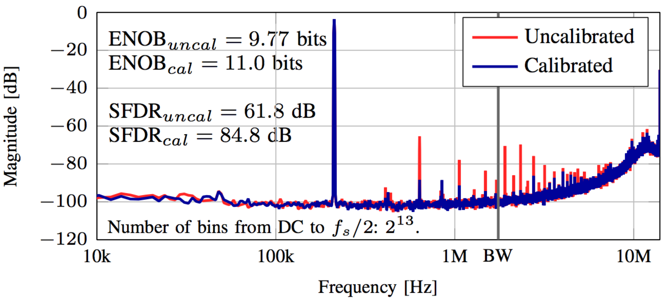
We will have a closer look at distortion, which is unwanted, or false signals that appear in the digital output because of imperfections in the circuit components. For instance, the ADCs we make contain a group of capacitors, which are components that store electric charge, exactly like water tanks store water. In this group, the next capacitor always has to be exactly twice as large as the previous one, such that they get the sizes 1, 2, 4, 8, 16, up to 512. In practice, this does not happen, because of inevitable inaccuracy in the production of integrated circuits. The result is an ADC that generates distortion and works poorly.
One solution to this problem is to make the capacitors very large, because they are then easier to produce. However, this come at the cost of much higher power consumption. A better solution is to use calibration, and digitally correct for the errors of the capacitor bank. We are working on two different calibration approaches. One is to measure the errors of the capacitors directly, and use the error measurements to correct the ADC output. For this method, we have made an ADC where a part of it can be configured to measure the capacitors when you power up the equipment. Afterwards, the ADC starts normal operation and use the measurements to correct its output.
In the other method, we have developed an algorithm that can estimate the capacitor errors just by looking at the distortion present at the ADC output. Specifically, we send a test signal (a sinusoid) into the ADC, and look at the digitized signal and distortion at the output. The algorithm then figures out what the capacitor errors inside the ADC have to be to make up exactly the distortion that we observe. Then we can use the errors, which are now estimated rather than measured, to correct the output signal.
